
Items list

Instead of dreaming big, some companies think small. Targeting IoT and embedded applications requiring a GUI and limited 3D capability, Think Silicon offers its NEMA®|p (“Pico”) and NEMA®|t (“Tiny”) licensable GPU cores as well as design tools to support rapid prototyping on FPGAs. NEMA®|p delivers 2/2.5D graphics for minimalist user interfaces in wearables and other small devices. NEMA®|t implements the industry standard Open Graphics APIs for low-power 3D rendering. RTL for both GPUs is available now. The company is additionally preparing a new design that targets heterogeneous processing, called NEMA®|S (“Small”), for release by 3Q17.
The company delivered the RTL for its NEMA®|p 2.5D GPU in 4Q15, winning a socket in the Sequans Monarch SX IoT processor (see MPR 4/17/17, “Sequans Adds CPU to IoT Modem”). The company has also won designs in Asian smartwatches for the elderly and children.
Think Silicon was founded in 2007 when several former Atmel engineers began developing display-controller intellectual property (IP) capable of compositing image layers and performing framebuffer compression in real time. Headquartered in Greece, co-founders George Sidiropoulos and Iakovos Stamoulis continue to serve as CEO and CTO, respectively. The company currently employs 25 people; 22 are engineers.
Think Silicon first dipped its toes into the GPU waters in 2012 by delivering the ThinkVG 2.5D core, which supported the OpenVG vector-graphics standard. Dialog Semiconductor used ThinkVG in its SC14453 Green VoIP MCU. Think Silicon works with distributor Tortuga Pacific to license its display controllers and GPU IP in North America. That company focuses on revenue generation, marketing assistance, and licensing for small IP companies.
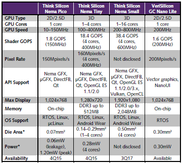
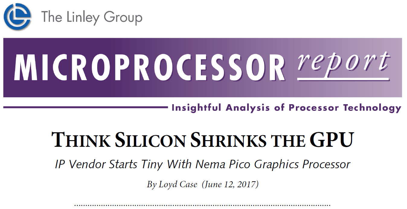
Table 1. Comparison of Think Silicon NEMA® and VeriSilicon GC Nano Lite GPUs. The VeriSilicon design is similar to the smallest Think Silicon GPU, NEMA®|pico. *All area and power numbers are for 28nm at maximum speed and include on-chip RAM. (Source: vendors)
IoT Needs Small GPUs
As IoT devices proliferate and become more sophisticated, they increasingly need GUIs. Although some systems may get by with simple LCD text displays, others need more attractive interfaces that provide more information. For example, a home-automation control panel may display HVAC status in real time, using sliders to dim lights, and show real-time power consumption graphs.
GPU-IP vendors have traditionally developed high-end products first, later decreasing die area and performance by removing features or reducing core count. For example, Imagination’s PowerVR Series8XE focuses on pixel throughput rather than fast polygon rendering, but it’s based on the PowerVR Series7. These downsized designs tend to offer more features and consume more area and power than simple IoT devices need.
Think Silicon has focused on embedded applications from the start, creating area-efficient designs fit for layered user interfaces and low-resolution 3D displays. It offers three GPU designs under the NEMA® brand, as Table 1 shows. RTL for NEMA®|p and NEMA®|t is available now; the first chips using these GPUs are scheduled to enter production later this year. The more powerful NEMA®|S (“Small”), which targets at heterogeneous-processing work-loads that require GPU-compute capability, is slated for production RTL release later this year and should appear in production chips by the end of 2018.
NEMA®|p leaks a scant 0.06mW compared with 0.3mW for VeriSilicon’s GC Nano Lite. IoT products often spend more time idle or sleeping than running, so low leakage is crucial for extending battery life. The 1.2mW peak power assumes a 150MHz clock speed, but because NEMA® supports dynamic voltage and frequency scaling (DVFS), designers can run it at a slower speed to save power.
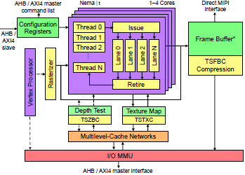
Figure 1. Block diagram of NEMA® architecture. NEMA®|p omits vertex processing and z-buffer features such as depth testing. *Resides in on-chip SRAM for NEMA®|p.
VLIW Architecture Accelerates Graphics
All three NEMA® GPUs employ a common architecture, shown in Figure 1. The engine uses a small VLIW instruction set and, in the case of NEMA®|t and NEMA®|S, is scalable to multiple lanes and cores. The three designs have the rasterizer, texture engine, frame-buffer-compression module, and general core in common. The architecture supports full cache coherence with other agents in the SoC. NEMA®|S offers important enhancements, including support for 16- and 32-bit floating point (FP16 and FP32).
All three models also implement proprietary framebuffer and texture compression. NEMA® GPUs employ Think Silicon’s 4-bits-per-pixel (4bpp) frame-buffer compression (TSFBC) for systems with limited memory and 6bpp TSFBC for high-resolution displays. Similarly, the company provides 4bpp and 6bpp texture compression (TSTXC). These techniques help squeeze the frame buffer and NEMA® libraries into the SoC’s on-chip memory, reducing the need for external framebuffer memory. In addition, NEMA®|t and NEMA®|S offer TSZBC for compressing z-buffers.
NEMA®|p implements a fixed-point data path and an instruction-set architecture (ISA) suitable for GUI and 2D graphics on small displays. The programmable shader core implements a quad-issue VLIW architecture and allows both 32-bit integer and 128-bit vector register types. The VLIW compiler detects and removes data dependencies, thereby simplifying the pipeline. At a typical speed of 150MHz (in 28nm HKMG technology), the core delivers a peak rate of 1.8 billion 8-bit integer operations per second (GOPS). To increase utilization, it implements up to 128 threads. When one thread stalls, the core immediately switches to another and continues to compute. This approach helps hide memory latency.
Back to the Basics
NEMA®|p lacks full 3D features such as depth testing and vertex processing but can do texture mapping, which is useful in multilayer 2.5D graphics. Tri-angles can be Gouraud shaded for more-pleasing color blending. Although NEMA®|p lacks z-buffer capability, the composition engine recognizes hidden areas in layers and avoids reading or drawing them. The GPU also has features typical of modern 2D accelerators, including multiple color formats, blitting, alpha blending, and perspective-correct image transformation.
Developers can use Think Silicon’s proprietary NEMA®|GFX, the open-source μGFX user interface, the DirectFB API, or Qt graphics APIs to create applications. NEMA®|t adds z-buffer support and vertex processing. It implements industry standard Open Graphics APIs.
As with NEMA®|P, it uses fixed-point math, so code developers must specify the OpenGL ES Common Lite profile. The tiny GPU comes in three flavors: the NEMA®|t-100, NEMA®|t-200, and NEMA®|t-400, which have one, two, and four cores respectively.
The NEMA® graphics pipeline consists of commands stored in the configuration register file (CRF) fed by the command processor. CRF subsets can be allocated to specific modules in the GPU cores as needed. The CRF can be memory mapped to the CPU address space, but writing directly to the CRF from the CPU is inefficient. Instead, the CPU collates command lists then feeds them to the command-list processor, as Figure 2 shows. Command lists are reusable, so the CPU needn’t recalculate repetitive tasks. NEMA®|S and NEMA®|t accept OpenGL programmable-shader code. The NEMA®|p pipeline behaves similarly but lacks depth-test capability.
The company builds power management into all levels of the architecture. Cores can power down indi-vidually. The hardware scheduler is designed to work with the power-management scheme, only feeding active cores. Dynamic voltage and frequency scaling (DVFS) applies individually at the core level. Framebuffer, z-buffer, and texture compression also reduce power by minimizing memory accesses.
Shrinking Heterogeneous Processing
Think Silicon’s plans for its first heterogeneous-processing GPU are ambitious. The upcoming NEMA®|S targets GPU-compute workloads and supports clusters of one to four cores. It fully supports many of the industry standard Open Graphics APIs. Unlike its predecessors, this GPU implements a unified-shader architecture that handles vertex, fragment, and GPGPU (general-purpose GPU) code. The NEMA®|S cores implement a floating-point data path that can execute one vector instruction and one scalar instruction per cycle. The vector unit can perform four multiply-add (MAD) FP16 operations on one lane while other operations run on other lanes. Operating at 533MHz, a four-core cluster can generate up to 19.2Gflop/s.
To further increase performance, NEMA®|S expands to 16 clusters, as Figure 3 shows. The clusters all share a set of local caches and optional hardware accelerators. Among these accelerators are a texture engine, texture mapper, pixel-blend unit, and polygon rasterizer. The clusters are linked by a proprietary network-on-chip (NoC) based on the well-known AXI fabric. In its maximum configuration, a 64-core NEMA®|S can generate 307Gflop/s while using just 8mm2 in 28nm. This performance is similar to that of an ARM Mali-G71 MP8 configuration that uses four times the die area.
In addition to graphics, NEMA®|S targets GPGPU computation, implementing OpenMP and OpenCL APIs.
Figure 2. NEMA® graphics-pipeline flow. Command lists contain graphics instructions that go to the configuration register file then to the GPU core.
Think Silicon offers a C/C++ LLVM compiler for directly programming the shader core. The shader compiler has prefetching capability that can keep the cores fed, improving both graphics and compute performance. NEMA®|S is also suitable for neural-network (NN) inferencing using FP16 weights, although many NNs are shifting to 8-bit integer math.
Designed Specifically for IoT
In the IoT space, VeriSilicon competes with Think Silicon by offering its GC Nano GPU IP. That design fits 2D, 2.5D, and light 3D workloads. As Table 1 shows, the NEMA®|p GPU consumes one-quarter the area and one-fifth the leakage power of the GC Nano Lite. ARM and Imagination scale down older GPUs for IoT. Imagination designed the GX5300, a slightly updated version of the PowerVR Series5 architecture, for area and power efficiency. ARM’s Mali-470 similarly builds on the older Mali-400 to target IoT and embedded graphics (see MPR 11/2/15, “Mali-470 Targets Wearables, IoT”). But neither of these alternatives comes close to NEMA®|p or NEMA®|t for small screens and basic GUIs.
Think Silicon designed its products for embedded and IoT systems needing user interfaces. This approach has led to tiny GPUs that consume much less power and die area than competitors. NEMA®|p and NEMA®|t deliver the right performance, area, and power balance for low-end IoT applications, increasing battery life and reducing costs.
NEMA®|S is more ambitious, aiming for IoT devices that require GPGPU, including augmented/virtual reality, neural-network inferencing for machine vision, and low-cost drones. Given the highly competitive market today for machine-learning accelerators, NEMA®|S has a tough road ahead, but it offers attractive performance per watt for these applications.
Price and Availability
NEMA®|p and NEMA®|t RTL is available now. Production RTL for NEMA®|S is scheduled to arrive in 3Q17. Think Silicon has not disclosed license fees. For details, access here.